
Share this
One-dimensional van der Waals heterostructures: Growth mechanism and handedness correlation revealed by nondestructive TEM
![]()
One-dimensional van der Waals heterostructures: Growth mechanism and handedness correlation revealed by nondestructive TEM
2021/09/16
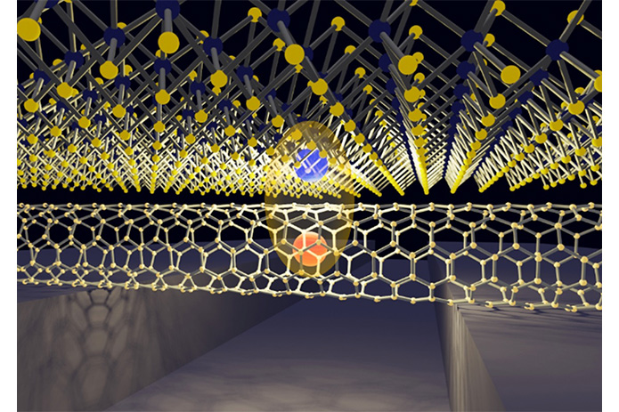
Large superconducting diode effect in ion-beam patterned Sn-based superconductor nanowire/topological Dirac semimetal planar heterostructures
Large superconducting diode effect in ion-beam patterned Sn-based superconductor nanowire/topological Dirac semimetal planar heterostructures
2024/10/01
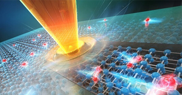
Room-temperature quantum emission from interface excitons in mixed-dimensional heterostructures
Room-temperature quantum emission from interface excitons in mixed-dimensional heterostructures
2024/04/12