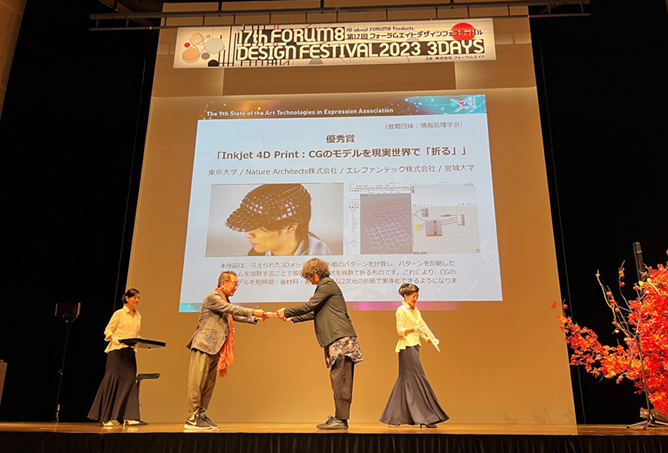
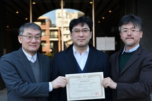
On 11th November 2021, Project Assistant professor Akio Higo, Project Researcher Yukinori Ochiai, and Associate Professor Yoshio Mita, Systems Design Lab (d.lab), recieved The Sensor and Micromachine Society of the Institute of Electrical Engineers in Japan 38th Sensor symposium Excellence Technical Paper Award.
The Sensor and Micromachine Society of the Institute of Electrical Engineers in Japan 38th Sensor symposium Excellence Technical Paper Award
This award is given to oral presentations over 36 years old with excellent research contents and presentations at the 38th Symposium on the Sensor Symposium at the Sensor and Micromachine Society of the Institute of Electrical Engineers in Japan. This year, nine finalists were announced on the first day of the symposium, then one best technical paper award and four excellent technical paper awards were selected. Most of the awards were given to companies themselves or to joint research groups between universities and companies. Our U-Tokyo group alone was only selected.
About awarded research
Nanogap with Concave Structure by Variable-shaped Beam/Character Projection Electron Beam Lithography
It is hard to realize the high throughput exposure by the point beam electron beam exposure systems. In contrast, the variable-shaped beam (VSB) method can realize the high throughput due to approximation of the rectangular shots, but it needs to overcome the nanogap issue about the nano-bridge. Our approach is to first realize pattern errors and then solve the issue one by one to realize the nanogap. In the near future, we will realize the method of accurate nanopatterns using machine learning.
Your impression & future plan
We are honored to receive this award for our recent research on nanostructure fabrication technology by high-speed and high-resolution electron-beam lithography technology. Among the racing for the semiconductor research field in the world, our research which is the development of the nanofabrication technology by using the character projection method in F7000S VD-02, Advantest corporation in Takeda Super Cleanroom with the MEXT nanotechnology platform and Advanced Research Infrastructure for Materials and Nanotechnology in Japan can lead the world in this field. We aim to realize the unique nanofabrication technology from U-Tokyo.
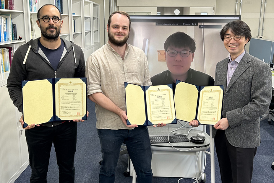
Benedikt Scholz (D3), Assistant Professor Yusuke Hayashi, Project Researcher Mohamed Rami Gaddem, Professor Hirokazu Sugiyama received Technical Achievement Award of SIS
Young Faculty : Project Associate Professor Kenji Shimazoe