〈Question〉
「Q」Please describe your presentation simply.
「A」We have developed an imaging technique using a CMOS camera to visualize the spatial distribution of microscopic physical properties in transparent materials that cannot ordinarily be optically observed. This technique has also successfully allowed us to see the non-uniform spatial distribution of electric polarizations in transparent optical materials.
「Q」Please tell us about the background for your research.
「A」CMOS cameras, which we also use daily in our smartphones, are semiconductor devices that convert optical images into electrical signals. In recent years CMOS cameras have improved dramatically, and research on materials science using that function is attracting attention. In particular, the modulation-imaging technique, a technique for visualizing the miniscule changes that occur when external fields are applied to an imaging target, can reveal the distribution of electric polarizations which cannot be seen in ordinary photography. Note that because conventional methods can only measure changes in the visible-light absorbance they are only applicable to colored materials, and thus cannot be used for measuring transparent materials.
「Q」Please tell us about the results you found.
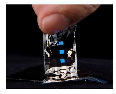
「A」By focusing on the electro-optic effect, in which an electric field slightly changes the refractive index of a material, we have developed the modulation-imaging technique, which can be applied to an expanded range of substances, which includes transparent materials. Although the intensity of the transmitted light remains the same when the refractive index of a material changes, the phase of the light changes. The response was very small, but the combination of CMOS camera and high-speed image processing units allowed us to succeed at once with high sensitivity to detect phase changes as miniscule as 0.01%. Using this technique, we also succeeded in making the non-homogeneous distribution of electric polarization in thin transparent insulator films visible in micrometer-scale detail.
「Q」Please tell us about forthcoming developments.
「A」These results have allowed us to expand modulation-imaging technique targets to a wider range of substances, including transparent materials. From now on, we would like to use this imaging technique to see the invisible and initiate a new movement in the study of materials science. As a matter of fact, based on our research, we have recently succeeded in seeing the distribution of clockwise and counterclockwise structures that have been thought to exist in functional metal-oxide crystals. Furthermore, in order to utilize CMOS cameras in new ways, we will continue to work on applications beyond the evaluation of materials characteristics and devices, and which can also be applied to a broader range of social issues.
For example, we would like to apply it as a tool for the advance detection of unseen dangers.
「Q」Please tell us how this research field is fascinating.
「A」The fascination in developing this kind of imaging technique is that it allows us to see things that have previously been invisible. When electrical measurements are taken, such as electric current, the information provided is an average within the material, but imaging technique allows us to know even more microscopic spatial distributions. Particularly, the use of light makes it possible not only to provide information about the surface of a material but also about its deep interior. We consider that the direct observation of the spatial distribution of a target of interest will lead to a more accurate and effective understanding of the material’s properties.
「Q」Please tell us about your usual routine.
「A」When conducting an experiment, I try to think of as many possible scenarios as possible in advance, including potential failure scenarios. I try to ensure that the experiment can proceed efficiently by being as prepared as possible for the unexpected situation. A system in place at the School of Engineering that allows students to work intensely on cutting-edge research in their respective fields, which I think is a very valuable opportunity. I think that immersing yourself in research and personally discovering a new phenomenon or creating a new is a special kind of fun that you can't experience with other activities. Therefore, I think tackling challenging topics head on and pursuing research that will deliver even greater joy is a good idea.
Authors
Yohei Uemura, Satoshi Matsuoka, Jun’ya Tsutsumi, Sachio Horiuchi, Shunto Arai, Tatsuo Hasegawa
Abstract
Observations of ferroelectric domains and domain walls are essential for understanding ferroelectric switching characteristics. Here, we demonstrate that the use of optical birefringence, coupled with a first-order electro-optic effect (Pockels effect), allows the visualization of ferroelectric domains in transparent ferroelectric materials. We utilize a field-modulation imaging technique, with the use of a complementary metal-oxide-semiconductor (CMOS) area image sensor to detect slight differences in parallel- and crossed-Nicols polarized optical microscopy images between forward- and reverse-electric-field applications. The ferroelectric domains with antiparallel polarizations are clearly discriminated from each other by the sign of the ellipticity modulation of outgoing elliptically polarized light. The observed images are consistent with piezoresponse force microscopy images of transparent single-crystal films of 2-methylbenzimidazole (MBI). The modulation signal at both polarization configurations exhibit clear sign changes in the wavelength dispersion, owing to the anisotropic nature of the MBI films. The unique optical-probe nature also reveals the existence of two types of domain walls with different three-dimensional orientations.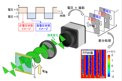
Physical Review Applied : https://journals.aps.org/prapplied/abstract/10.1103/PhysRevApplied.14.024060