
Share this
Ultrafast Subpicosecond Magnetization of a 2D Ferromagnet
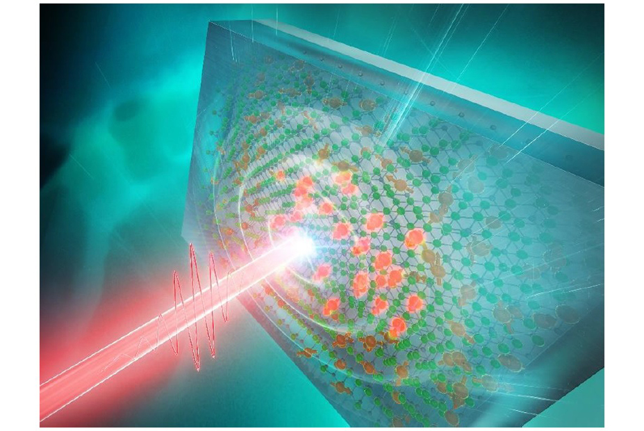
Ultrafast Subpicosecond Magnetization of a 2D Ferromagnet
2023/08/01
Giant spin-to-charge conversion at an all-epitaxial single-crystal-oxide Rashba interface with a strongly correlated metal interlayer
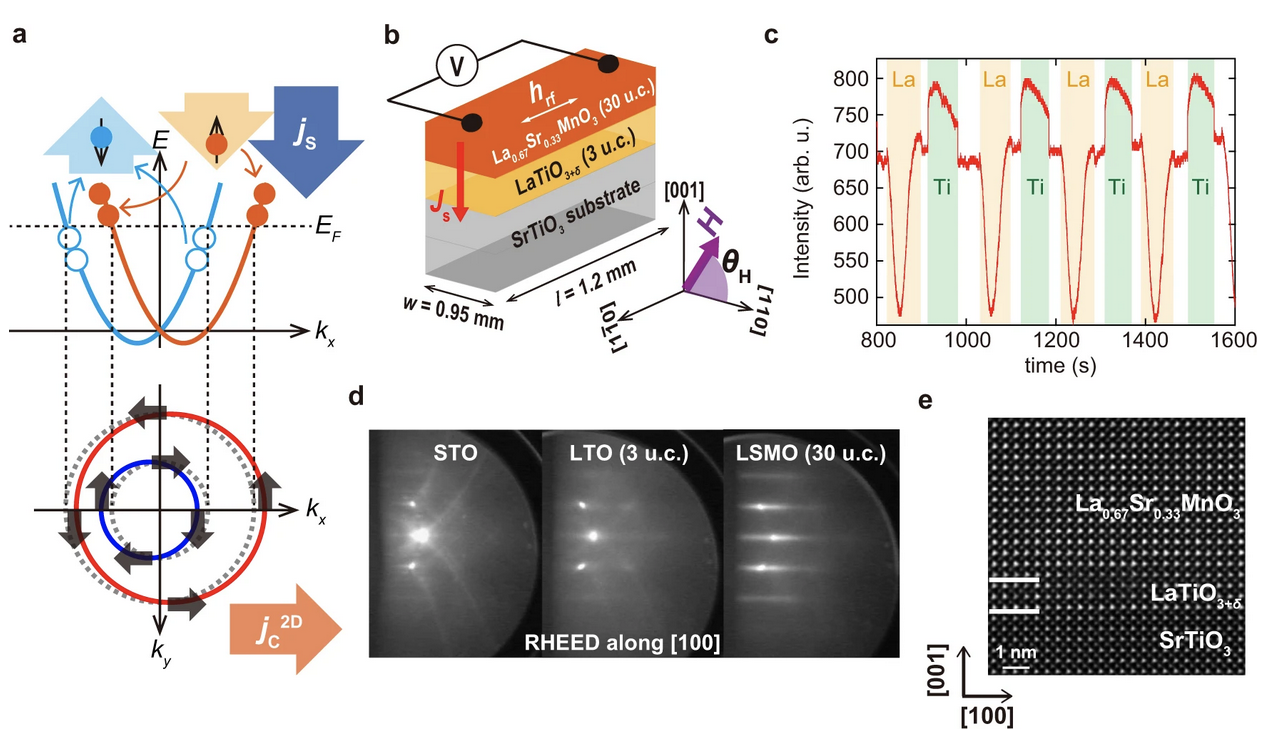
Giant spin-to-charge conversion at an all-epitaxial single-crystal-oxide Rashba interface with a strongly correlated metal interlayer
2022/10/04
Quantum phase transitions in highly crystalline two-dimensional superconductors
![]()
Quantum phase transitions in highly crystalline two-dimensional superconductors
2018/02/22