For devices such as smart watch and AR/VR equipment, the addition of AI functionality can significantly enhance user experience by enabling sophisticated vital analysis to improve quality of life (QOL), and by improving ease-of-use of the device, and so forth. However, such IoT devices need to be compact and lightweight, which requires them to be battery-powered, in addition to being low cost. Various AI processor technologies have been developed around the world to achieve lower power operation, but they all require the development of photomasks which cost on the order of US$10 million, presenting a high barrier to adoption by IoT devices. The unit price of the chip must be set high to recoup the development costs, which discourages adoption.
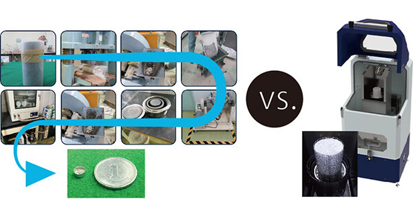
In this research, we developed a novel, structured ASIC-based AI processor which achieves both low power operation and low cost. Chips are first prefabricated with processing circuitry and partially formed routing layers. Then, using our newly developed via-programmable neuron array technology, we can form the AI processor circuitry that performs specific AI processing by customizing only the top VIA1 layer. This allows us to significantly slash the AI processor fabrication costs by reducing the number of photomask layers to just one for the VIA1 layer. The biggest challenge in realizing this technology was the large implementation area. Using conventional approaches, the implementation of wired logic-based deep neural networks (DNNs) requires a tremendous amount of signal wires. The resultant area greatly exceeds the manufacturable size of an IC, making it unrealizable. Our research team developed a bit- and neuron-serial circuit technology which slashes circuit area by utilizing time-shared reuse of both circuit and wiring. In addition, we developed a function-selective non-linear neural network (FS-NNN) technology which reduces the bit width of DNN weight coefficients from 16 bits (for 65,536 values) to 3 values (+1, -1, 0) without sacrificing accuracy, thereby significantly reducing the number of signal wires required. By combining these novel technologies, we succeeded in slashing the number of wires by a factor of 1/1024 to reduce circuit area to within 10mm2, which is small enough for us to realize AI functionality in a structured ASIC for IoT applications. We expect this to be applicable to not only wearable IoT devices, but also drones, in-vehicle entertainment system control panels, and AR/VR equipment.

Papers
Conference: International Solid-State Circuits Conference(ISSCC)
Title: A Via-Programmable DNN-Processor Fabrication Toward 1/40th Mask Cost
Authors: Jaewon Shin, Rei Sumikawa, Dong Zhu Li, Mototsugu Hamada, Atsutake Kosuge*
Development of "slow" but efficient information processing technology: Successful demonstration of low-power transistor mimicking biological neuron behavior

For the development of Environmental-Friendly Waterborne Paintings: Molecular-Scale Simulations for Film Formation of Waterborne Paintings