Authors
Y. J. Zhang*, T. Ideue, M. Onga, F. Qin, R. Suzuki, A. Zak, R. Tenne, J. H. Smet, and Y. Iwasa
Abstract
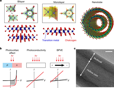
The photovoltaic effect in traditional p–n junctions—where a p-type material (with an excess of holes) abuts an n-type material (with an excess of electrons)—involves the light-induced creation of electron–hole pairs and their subsequent separation, generating a current. This photovoltaic effect is particularly important for environmentally benign energy harvesting, and its efficiency has been increased dramatically, almost reaching the theoretical limit. Further progress is anticipated by making use of the bulk photovoltaic effect (BPVE), which does not require a junction and occurs only in crystals with broken inversion symmetry. However, the practical implementation of the BPVE is hampered by its low efficiency in existing materials. Semiconductors with reduced dimensionality or a smaller bandgap have been suggested to be more efficient. Transition-metal dichalcogenides (TMDs) are exemplary small-bandgap, two-dimensional semiconductors in which various effects have been observed by breaking the inversion symmetry inherent in their bulk crystals, but the BPVE has not been investigated. Here we report the discovery of the BPVE in devices based on tungsten disulfide, a member of the TMD family. We find that systematically reducing the crystal symmetry beyond mere broken inversion symmetry—moving from a two-dimensional monolayer to a nanotube with polar properties—greatly enhances the BPVE. The photocurrent density thus generated is orders of magnitude larger than that of other BPVE materials. Our findings highlight not only the potential of TMD-based nanomaterials, but also more generally the importance of crystal symmetry reduction in enhancing the efficiency of converting solar to electric power.