
Authors
Satoshi Anada, Kazuo Yamamoto, Hirokazu Sasaki, Naoya Shibata, Yujin Hori, Kouhei Kinugawa, Akihiro Imamura & Tsukasa Hirayama
Abstract
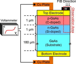
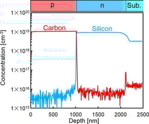
We combined an in situ biasing technique with phase-shifting electron holography, which can simultaneously achieve a high precision and high spatial resolution, to measure the electric potential, field, and charge density profiles across a GaAs p-n tunnel junction. A thin-film specimen was prepared by thinning one part of a bulk specimen using a cryo focused ion beam (FIB) system. We obtained precise electric potential profiles and successfully converted them into smooth electric field and charge density profiles without any fitting simulations. From the relationship between the applied voltage and measured height of the potential step across the p-n junction, the built-in potential of the p-n junction was determined to be 1.55 ± 0.02 V. The electric field profiles showed that the unbiased p-n junction had a depletion layer with a width of 24 ± 1 nm; the width increased to 26 ± 1 nm under a reverse bias of −0.3 V and decreased to 22 ± 1 nm under a forward bias of 0.5 V. Moreover, the charge density profiles indicated the presence of passivated dopants and/or trapped carriers even in the internal active layer of the specimen, with little damage introduced by FIB milling.
Journal of Applied Physics : https://aip.scitation.org/doi/full/10.1063/1.5006837
Japan Fine Ceramics Center: http://www.jfcc.or.jp/en/
Share this
Electrode potential influences the reversibility of lithium metal anodes
Electrode potential influences the reversibility of lithium metal anodes
2022/10/28
Hydrate-melt electrolytes for high-energy-density aqueous batteries
![]()
Hydrate-melt electrolytes for high-energy-density aqueous batteries
2016/08/28
Strong-correlation induced high-mobility electrons in Dirac semimetal of perovskite oxide
![]()
Strong-correlation induced high-mobility electrons in Dirac semimetal of perovskite oxide
2019/01/24