
Authors
Thanh-Hung Dinh, Nikita Medvedev, Masahiko Ishino, Toshiyuki Kitamura, Noboru Hasegawa, Tomohito Otobe, Takeshi Higashiguchi, Kazuyuki Sakaue, Masakazu Washio, Tadashi Hatano, Akira Kon, Yuya Kubota, Yuichi Inubushi, Shigeki Owada, Tatsunori Shibuya, Beata Ziaja & Masaharu Nishikino
Abstract
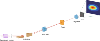
Interaction of a solid material with focused, intense pulses of high-energy photons or other particles (such as electrons and ions) creates a strong electronic excitation state within an ultra-short time and on ultra-small spatial scales. This offers the possibility to control the response of a material on a spatial scale less than a nanometer—crucial for the next generation of nano-devices. Here we create craters on the surface of a silicon substrate by focusing single femtosecond extreme ultraviolet pulse from the SACLA free-electron laser. We investigate the resulting surface modification in the vicinity of damage thresholds, establishing a connection to microscopic theoretical approaches, and, with their help, illustrating physical mechanisms for damage creation. The cooling during ablation by means of rapid electron and energy transport can suppress undesired hydrodynamical motions, allowing the silicon material to be directly processed with a precision reaching the observable limitation of an atomic force microscope.
Communications Physics : https://www.nature.com/articles/s42005-019-0253-2