PRESS RELEASE
- Research
- 2020
Influence of interlayer stacking on gate-induced carrier accumulation in bilayer MoS2
Authors
Mina Maruyama, Kosuke Nagashio, Susumu Okada
Abstract
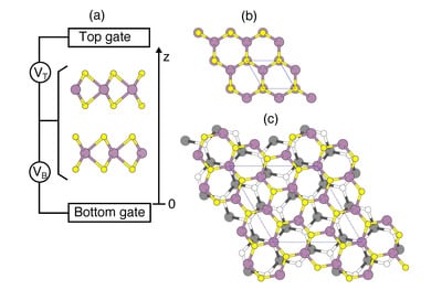
Atomic layered materials with a semiconducting electronic property have attracted much attention as a conducting channel in field effect transistors (FETs). Here, we investigate the electronic structures of bilayer MoS2 in a dual gate FET model by using first-principles total-energy calculations based on the density functional theory. Our calculations show that selective electron doping occurs in bilayer MoS2 under a perpendicular electric field owing to a band-offset between the positive and negative electrode sides of the MoS2 layers. Furthermore, we observe a further partial carrier distribution in bilayer MoS2 by decreasing the inter-layer interaction owing to a twisted stacking arrangement. It is expected that the positive-electrode-side layer works as a conducting channel, on the other hand, the negative-electrode-side layer works as a screening layer in bilayer MoS2-FET.
ACS Applied Electronic Materials:https://pubs.acs.org/doi/abs/10.1021/acsaelm.0c00139